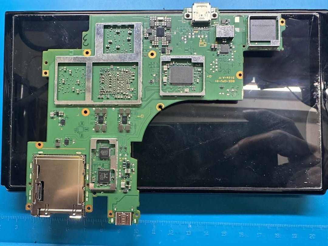
Certainly, the Nintendo Switch 2 is one of the most highly awaited gaming consoles. With the recent rumors about the chip powering the console called T239, discussions surrounding the performance and efficiency have fired up. Although there has been some skepticism regarding the adoption of Samsung’s 8nm process node used for chip manufacturing with regard to power efficiency and battery life, many experts believe that this hardly impacts the power of the console. Here is an in-depth look into it.
T239 Chip: A Detailed Explanation
Digital Foundry recently did an in-depth look at the rumored Nintendo Switch 2 motherboard, where their focus lay in the T239 system-on-chip. With most of the other components being run-of-the-mill, this one chip seems to be drawing quite a lot of attention simply for its anomalous specifications.

Samsung’s 8nm Process Node
Speculations are being made by professionals that the T239 chip is manufactured based on Samsung’s 8nm process node, basing this fact on how it has quite a lot of similarities with its sibling chip, the T234, which uses an 8nm node as well. Secondly, the 8nm is precisely the node on which NVIDIA’s Ampere architecture in T239 was targeted, and shifting down to 4nm, for example, would be illogical if the underlying architecture were not changed to Lovelace, fitting best at 4nm.
While Samsung’s 5nm process is another possibility, porting the Ampere architecture over to that node would require substantial redesign efforts. Besides, Samsung’s 8nm process is considerably cheaper owing to its relatively rare utilization in current devices, fitting Nintendo’s hardware development philosophy of keeping costs low.
The 8nm node was thought to be too power hungry, but this is not believed to be an issue, at least for the T239 chip, because of particular design optimizations which will let it overcome those challenges.
Differences with the T234 Chip
While the T239 derives from the T234, it does not represent its straightforward shrink. The architecture and features between the two chips differ. In many ways, it is obvious that the T239’s target is gaming because of added elements such as a file decompression block for faster load times and easier asset management. It is smaller and less power-hungry compared to T234, which gives hints about optimization in the process towards portable gaming.
Power Efficiency Objectives
By the looks of a leaked motherboard with a rather small battery cavity, the T239 chip was probably designed keeping power efficiency in mind. This goes to say that performance and battery have been kept balanced by deliberate efforts from Nintendo. While the attainment of complete efficiency on an 8nm node is somewhat hard to achieve, the design of the chip has remarkably toned down these limitations

Leaked Features and Possible Innovations
The T239 chip isn’t the only intriguing aspect of the Nintendo Switch 2 leaks. Recent images of the system’s Joy-Con controllers hint at potential new functionalities.
Joy-Con as a PC Mouse?
The newly designed Joy-Con controllers boast additions suggesting they could be used as a PC mouse. This begs the question of whether this is going to be the system’s feature or just an optional upgrade. Details are, of course, still slim, but this has caught the interest of many fans who are just ready for Nintendo to wow them with its next-generation console.
Conclusion
The T239 chip of the Nintendo Switch 2, fabricated on an 8nm process node by Samsung, is finally taking center stage in the system. While power efficiency and performance concerns remain, the design of the chip shows that it will handle modern gaming quite well. Paired with possible innovations such as enhanced Joy-Con, the Nintendo Switch 2 seems like an interesting addition to the gaming world. Won’t have to wait much longer to see these features come together as more details will arrive soon.
